The Science of Defect Engineering via Chemically Active Surfaces
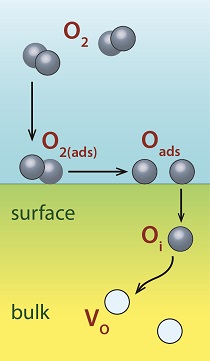
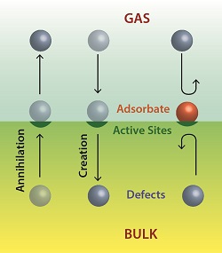
In the same way that gases react with surfaces from above, solid defects can react from below. Figure 1 shows an example of molecular gaseous oxygen breaking apart on a metal oxide surface, which in turn injects oxygen interstitials (Oi) into the bulk to eliminate oxygen vacancies (Vo) that reside there. Little attention has been paid to this form of surface chemistry up to now. Yet as devices shrink and surface-to-volume ratios increase, surface phenomena become increasingly important, and surface-based defect engineering strategies become more viable. Our basic idea is that making surfaces more chemically active by removing passivation can controllably increase the annihilation rate (or injection/creation rate, depending upon the application) of defects at that surface. Figure 2 depicts this idea schematically, showing both creation and annihilation of defects at active sites, as well as inhibition of annihilation at active sites that are passivated with an adsorbate.
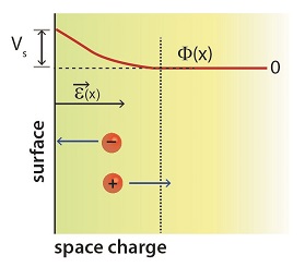
Since defects can be electrically charged, electric fields that often exist near surfaces can also be manipulated (Fig. 3) to attract or repel charged defects nearby. We employ optical methods to measure these electric fields.
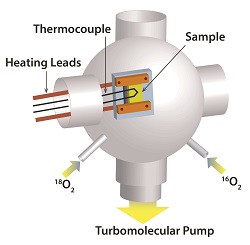
To better understand all these phenomena, we make indirect measurements of defect concentrations by monitoring solid-state diffusion rates in the vicinity of surfaces. Atomic defects themselves are very difficult to see directly, but the diffusion rate of an isotope or dopant generally scales with defect concentration. Typical experiments involve exposing single crystal surfaces of semiconductors such as TiO2 or ZnO to isotopically labeled oxygen gas. Fig. 4 depicts a typical experimental apparatus, which employs an ultrahigh vacuum (UHV) chamber. The gas atoms exchange through the surface with oxygen atoms in the bulk, and we measure the rate of this diffusional exchange with secondary ion mass spectrometry. We are performing loosely analogous experiments with isotopic titanium to understand how the metal-related defects behave.
To interpret the diffusion results, we have developed several mathematical models for the diffusion in metal oxides. These models involve the solution of differential equations describing defect diffusion and reaction.
To supplement this work, we also perform quantum calculations (in collaboration with Prof. Elif Ertekin on campus) to uncover the atomistic pathways and energies associated with defect injection and annihilation. Fig. 5 shows an example from a calculation for oxygen interstitial injection into ZnO.
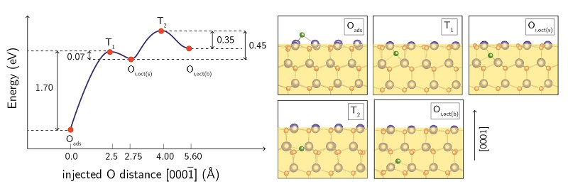
Fig.5
Applications: Oxide Heterosturctures for Catalysis and Photocatalysis
The discussion above outlines how surface chemistry affects the behavior of defects in the underlying semiconductor. Yet the reverse is also true - the defect-induced electronic properties of the solid can influence surface reactivity. Examples include surface-active "devices" such as certain catalysts and sensors. We seek to exploit such effects in metal oxide heterostructures, in which one semiconducting oxide is supported on another. Such supported oxides are widely used in industry for production of chemical products (oxidation of alcohols, oxidative dehydrogenation of alkanes) and for environmental cleanup (selective catalytic reduction of NOx in large-scale combustion flues). Through the synthesis methods described above, we seek to tune the activity and selectivity of supported catalysts. One example is vanadia (V2O5) supported on titania (TiO2). Another is titania supported on strontium ruthenate (Sr2RuO4) for photocatalysis. The reactivity of the overlayer can be tuned by changing the charge carrier concentration in the underlayer. We therefore grow thin films of the overlayer by atomic layer depositions or variants of that technique. Then we make reaction rate measurements of well-understood model reactions in a small reactor.
For this work, we synthesize films of TiO2 (in its anatase form) that are only 30 to 300 nm thick. The synthesis method we employ is atomic layer deposition, in which a solid substrate is exposed to alternating flows of source gases to build up a thin film one atomic layer at a time. For TiO2, we use Ti(OCH(CH3)2)4 to provide titanium and H2O to provide oxygen. Fig. 6 shows a schematic diagram of the setup, along with a typical grown specimen. Fig. 7 shows what the material looks like on a length scale of micrometers.
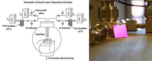
Fig.6
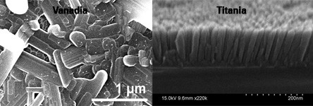
Fig.7
Once the material is grown, we subject it to a powerful battery of physical, chemical, and electrical characterization techniques to understand the nature of the oxide that has formed. Methods include X-ray photoelectron spectroscopy (XPS), X-ray diffraction (XRD), X-ray reflectivity (XRR), and scanning electron microscopy (SEM) to understand film composition, structure, and morphology. We determine electrical properties by measuring film capacitance as a function of applied voltage in a special diode test structure. The method is complicated but provides rigorous and accurate determination of TiO2 carrier concentration, which we correlate to the performance of a catalyst or sensor.
Recently, we have started to adapt such methods to make conventional porous particulate-based catalysts and photocatalysts instead of solid thin films.
|